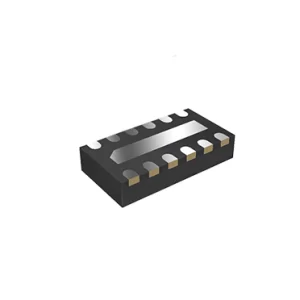
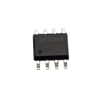
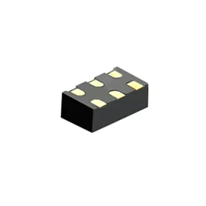
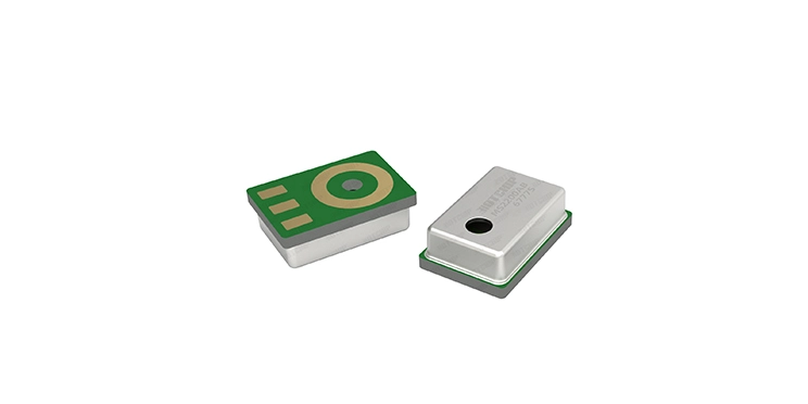
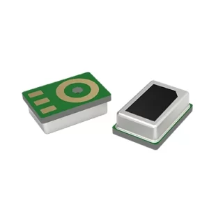
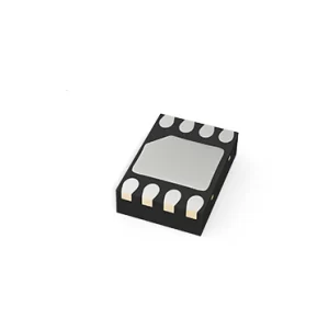
MS2203AB-M08 features a ASIC design, there will not be the current MCU program’s crash phenomenon, nor will there be below the critical voltage caused by the chip can not be reset phenomenon; power-saving mode quiescent current ≤ 5uA, peripheral application circuit is simple.
This product features a compact 2.7×1.8mm package suitable for SMT applications and supports high-efficiency automated production.
1. Specification Parameters
| Symbol | Parameter | Condition | Min. | Typ. | Max. | Unit |
| P | Operating Pressure | -150 | / | -250 | Pa | |
| Vdd | Operating Voltage Range | 2.4 | 3.7 | 5.0 | V | |
| Iq | Static Current | / | 2 | 5 | uA | |
| T-EN | Output Startup Time | / | 30 | 100 | mS | |
| Vol | Output Low Voltage | VDD=3.7V,Io=10mA | VDD*15% | V | ||
| Voh | Output High Voltage | VDD=3.7V,Io=10mA | VDD*85% | V | ||
| tONM | Smoking Protection Time | 12 | S |
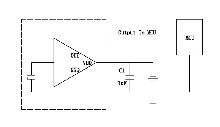
2. Typical Application Circuit Diagram
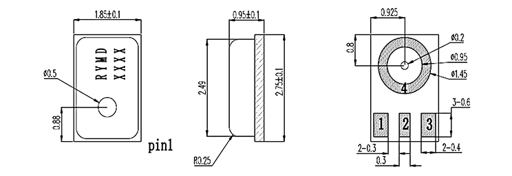
3. System Diagram
(1) System Structure Diagram
Unit: mm, Unmarked Tolerance: ± 0.1(mm)
| ITEM | DIMENSION | TOLERANCE | UNITS |
| LENGTH(L) | 2.70 | ±0.10 | mm |
| WIDTH(W) | 1.80 | ±0.10 | mm |
| HEIGHT(H) | 0.95 | ±0.10 | mm |
| AP1 | Φ0.20 | ±0.05 | mm |
| AP2 | Φ0.50 | ±0.05 | mm |
| Pin | Pin Name | Description |
| 1 | NC | / |
| 2 | Output | Switch output |
| 3 | VDD | Power supply |
| 4 | GND | Ground |
Note: All Ground Pin must be connected to the ground in end application.
(2) Installation Diagram
