1. Specifications
Unless otherwise specified, all parameters are measured at room temperature and referenced to the GND pin as the zero potential.
| Parameters | Symbol | Condition | Min. | Typ. | Max. | Unit | ||
| Charging System | ||||||||
| Input Voltage | VIN | 4.75 | 5 | 5.5 | V | |||
| Full State Input Current | IVIN | VIN=5V,BTP=4.2V
Indicator Current Not Included |
1 | 2 | mA | |||
| Charging Target Voltage | VTRGT | VSET Floating | 4.18 | 4.22 | 4.26 | V | ||
| Charging Current | ICHRG | VIN Pin | 2.1 | A | ||||
| Trickle Charging Current | ITRKL | VIN=5v,BAT=2.0v | 90 | 120 | 150 | mA | ||
| Trickle Cutoff Voltage | VTRKL | 2.9 | 3 | 3.1 | V | |||
| Recharging Threshold | VRCH | 4.06 | 4.1 | 4.14 | V | |||
| Charging Deadline | TEND | 20 | 24 | 27 | Hour | |||
| Input Overvoltage Protection | Vovp_ch | 5.55 | 5.7 | 5.85 | V | |||
| Input Overvoltage Hysteresis | Vovp_hys | 100 | mV | |||||
| Input Undervoltage Protection | VUVLO | Rising Voltage | 4.4 | 4.5 | 4.6 | V | ||
| Undervoltage Protection Hysteresis | VUVLO | 200 | mV | |||||
| Boost System | ||||||||
| Battery Operating Voltage | VBAT | 2.8 | 4.4 | V | ||||
| Switch Operating Battery Input Current | IBAT | VBAT=3.7V, VOUT=5.1V,
Indicator Current Not Included |
4 | mA | ||||
| DC Input Voltage | VOUT | VBAT=3.7V @0A | 5.0 | 5.10 | 5.20 | V | ||
| VBAT=3.7V @3.4A | 4.8 | 5.18 | V | |||||
| Output Voltage Ripple | ΔVOUT | VBAT=3.7V, VOUT=5.0V,
fs=500KHz |
100 | mV | ||||
| Booster System Supply Current | Ivout | 3.4 | 3.8 | 4.2 | A | |||
| Load Overcurrent Detection Time | TUVD | The output voltage remains consistently below 4.2V | 3.5 | 5 | 6.5 | ms | ||
| Load Short Circuit Detection Time | TOCD | The output voltage remains consistently below 2V | 150 | 200 | us | |||
| Control System | ||||||||
| Switch Frequency | fs | Switch Frequency | 450 | 500 | 550 | KHz | ||
| PMOS On-resistance | Rdson | 10 | 15 | 25 | mΩ | |||
| NMOS On-resistance | 10 | 15 | 25 | mΩ | ||||
| Battery Input Standby Current | ISTB | VIN=0V,VBAT=3.7V | 50 | uA | ||||
| LED Lighting Drive Current | Ilight | 20 | 30 | 40 | mA | |||
| LED Display Drive Current | IL1 IL2 IL3 | 3 | mA | |||||
| Auto Shutdown Load Current | Iauto_off | 60 | mA | |||||
| Load Auto-Detect Time | TloadD | Load current continuously less than 40mA | 27 | 32 | 37 | s | ||
| Short Keystroke Wake-Up Time | TOnDebounce | 30 | 50 | 500 | ms | |||
| Turn on Light Time | TKeylight | 1.2 | 2 | 3 | s | |||
| Thermal Shutdown Temperature | TOTP | Rising Temperature | 140 | ℃ | ||||
| Thermal Shutdown Temperature Hysteresis | ΔTOTP | 40 | ℃ | |||||
2. Product Features
Synchronous Charging and Discharging
3.4A synchronous boost conversion and 3A synchronous switching charging, with a boost efficiency of up to 95% and CC/CV output charging efficiency of up to 93%. The three-stage charging system has built-in power path management, supporting simultaneous charging and discharging, as well as a low-current discharge mode.
Charging
Adaptive charging current adjustment to match all adapters, supporting 3A charging via TYPE-C and 2A via MICRO B. The TYPE-C port can only be used with adapters to prevent incorrect discharging from DRP devices. It supports battery voltages of 4.20V, 4.30V, 4.35V, and 4.40V and includes battery temperature NTC protection.
Battery Indicator
Supports 4/3/2/1 LED battery indicators, with a programmable battery level curve for more uniform indicator lighting.
Feature-Rich
Automatically detects phone insertion and removal. Integrates TYPE-C DRP protocol, supporting single-port input and output, and features load large-current line compensation. It also supports dual-channel phone charging with intelligent DCP recognition.
Low Power Consumption
Intelligent load detection with automatic standby mode.
Simplified BOM
Integrated power MOS and single inductor for charging and discharging, with a 500kHz switching frequency, supporting a 1uH inductor.
Comprehensive Protection and High Reliability
Includes output overcurrent, overvoltage, and short-circuit protection, as well as input overvoltage, overcharge, overdischarge, and overcurrent discharge protection. The system also features over-temperature protection, battery NTC temperature protection, 4KV ESD protection, and an 11V surge withstand voltage.
Customized Solutions
I2C interface allows flexible and cost-effective custom solutions.
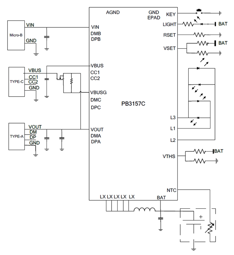
3. Typical Application Circuit Diagram
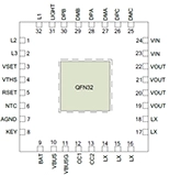
4. Pin Diagram and Functional Description
| Pin Name | Pin Number | Functional Description | |
| L2 | 1 | Power Indicator Drive Pin L2, functions as SDA in I2C mode | |
| L3 | 2 | Power Indicator Drive Pin L3, functions as MCU wake-up pin in I2C mode | |
| VSET | 3 | Battery Type Setting, options: 4.20V / 4.35V / 4.40V | |
| VTHS | 4 | Battery Platform Selection | |
| RSET | 5 | Battery Internal Resistance Compensation, allows fine-tuning of the battery level curve | |
| NTC | 6 | Temperature sensitive resistor detection pin | |
| AGND | 7 | Analog Ground | |
| KEY | 8 | Key Input Pin | |
| BAT | 9 | Boost Input Pin, connected to the positive terminal of the lithium battery | |
| VBUS | 10 | VBUS Charging Power Detection Pin | |
| VBUSG | 11 | VBUS Charging Input PMOS Control Pin | |
| CC1 | 12 | TYPE-C Detection Pin CC1 | |
| CC2 | 13 | TYPE-C Detection Pin CC2 | |
| LX | 14-18 | DC-DC Switching Node, connected to inductor | |
| VOUT | 19-22 | 5V Output Pin | |
| VIN | 23-24 | 5V Input Pin | |
| DMC | 25 | Output DCP D1- | |
| DPC | 26 | Output DCP D1+ | |
| DMA | 27 | Output DCP D0- | |
| DPA | 28 | Output DCP D0+ | |
| DMB | 29 | Input DCP D- | |
| DPB | 30 | Input DCP D+ | |
| LIGHT | 31 | Flashlight Drive Pin, open-drain output | |
| L1 | 32 | Power Indicator Drive Pin L1, functions as SCL in I2C mode | |
| EPAD | 33 | Power Ground and Thermal Ground, requires good contact with GND |
5. Features
- Charging Management Module.
- Boost Converter Module.
- Simultaneous Charging and Discharging.
- Indicator Lights Funtion.
- Flashlight Control Function.
