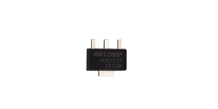
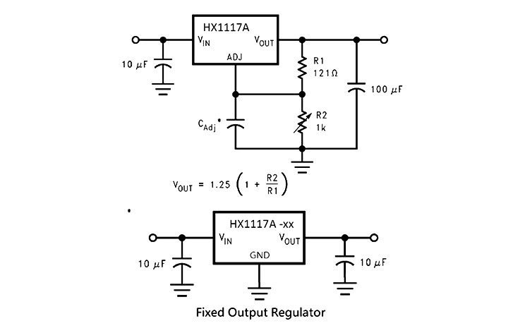
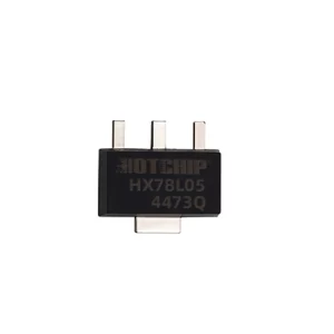
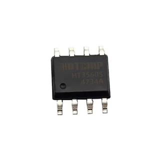
The HX1117 features an adjustable version that allows the output voltage to be set between 1.28 V and 13.8 V using two external resistors. Additionally, it is available in five fixed voltage options: 1.8 V, 2.5 V, 3.3 V, and 5 V. The HX1117 provides current limiting and thermal shutdown protection. Its circuit includes a Zener-trimmed bandgap reference to ensure output voltage accuracy within ±1%. A minimum output capacitor of 10 μF is required to enhance transient response and stability. The HX1117 is available in TO252, SOT223, and SOT-89 packages.
1. Specifications
| Parameter | Symbol | Condition | Min. | Typ. | Max. | Unit |
| Reference Voltage (adjustable version) |
VREF | VIN-VOUT=2V, IOUT=10mA | 1.232 | 1.25 | 1.268 | V |
| VIN-VOUT=1.4~10V, IOUT=10~800mA | 1.225 | 1.275 | ||||
| Output Voltage ( fixed version) |
VOUT | VIN= VOUT +2V, IOUT=10mA | Vo*0.985 | Vo | Vo*1.015 | V |
| VOUT +2V <VIN<10V,IOUT=10~800mA | Vo*0.98 | Vo*1.02 | ||||
| Static Current | IQ | TJ = 25℃ | 2 | mA | ||
| TJ = 125℃ | 5 | |||||
| Return Voltage | VDROP | IOUT=100mA | 1.2 | V | ||
| IOUT=500mA | TBD | |||||
| IOUT=800mA | TBD | |||||
| Ripple Rejection | PSRR | f = 120Hz, VIN = VOUT +3V | 75 | dB | ||
| Output Noise Voltage | VN | f = 10Hz to 100KHz | 0.004 | % | ||
| Adjust Pin Current | IADJ | 60 | 120 | uA | ||
| Thermal SD | TSD | 150 | C | |||
| Output Current Limit | ILIMIT | 1.1 | 1.5 | A |
2. Product Features
- Available in 8 V, 2.5 V, 3.3 V, 5 V and adjustable versions.
- Current limiting and thermal protection.
- Output current 800 mA.
- Line regulation: 2% (max).
- Load regulation: 4% (max).
- Available in SOT-223, TO252, SOT-89 packages.
3. Typical Application Circuit Diagram
4. Pin Diagram and Functional Description
| Pin Name | Pin Number(TO252) | Pin Number(SOT223) | Functional Description |
| INPUT | 1 | 1 | Input Voltage Pin |
| OUTPUT | 2,TAB | 2,TAB | Output Voltage Pin |
| ADJ/GDN | 3 | 3 | Ground |
