

1. Specifications
VIN = 3.7V, CTRL = 3.7V, VPOS = +4.6V, VNEG = -2.2V, typical value at TA = 25°C (unless otherwise specified).
| Symbol | Parameters | Condition | Min. | Typ. | Max. | Unit |
| General | ||||||
| VIN | Power Supply Input Voltage | 2.9 | 3.7 | 4.5 | V | |
| Temp | Operating Temperature | -40 | 25 | 85 | ℃ | |
| ISD | Shutdown Current | CTRL=GND | 1 | µA | ||
| VUVLO | Undervoltage Lockout Threshold | VIN Falling | 2.1 | V | ||
| VIN Rising | 2.3 | |||||
| Logic Signal (CTRL) | ||||||
| VH | High Threshold | VIN=2.9 to 4.5V | 1.2 | V | ||
| VL | Low Threshold | 0.4 | ||||
| RDOWN | Pull-Down Resistance | 300 | kΩ | |||
| Boost Converter (VPOS) | ||||||
| RDS(on)1A | Switch On-Resistance | ISWP1=200mA | 200 | mΩ | ||
| RDS(on)1B | Rectifier On-Resistance | 350 | ||||
| fSW1 | Switching Frequency | IVPOS=200mA | 1.5 | MHz | ||
| ISW1 | Switch Current Limit | Inductor peak current | 0.6 | A | ||
| IO1MAX | Maximum Output Current | VIN=2.9V to 4.5V | 200 | mA | ||
| VSCP1 | Short Circuit Threshold During Operation | VPOS falling | 85% of VPOS | |||
| RDCHG1 | Discharge Resistance | CTRL=GND, ISWP1=1mA | 30 | Ω | ||
| Inverting Converter (VNEG) | ||||||
| VNEG | Output Voltage Default | -2.2 | V | |||
| Output Voltage Range | -1.4 | -4.4 | ||||
| Output Voltage Accuracy | 25°C≤TA≤ 85℃ No load | -50 | 50 | mV | ||
| –30°C≤TA≤ 85℃ No load | -60 | 60 | ||||
| Line Regulation | IVNEG=200mA | 0.01 | %/V | |||
| Load Regulation | 0.1 | %/A | ||||
| RDS(on)2A | SWN MOSFET On-Resistance | ISWN=200mA | 200 | mΩ | ||
| RDS(on)2B | SWN Rectifier On-Resistance | 300 | mΩ | |||
| IO2MAX | Maximum Output Current | VIN=2.9V | 200 | mA | ||
2. Product Features
- Operating Input Voltage Range from: 2.9V to 4.5V.
- Boost Converter (VPOS).
(1) 4.6V Output Voltage;
(2) 200mA Output Current;
(3) 0.5% Accuracy (25°C to 85°C).
- Inverting Converter (VNEG).
(1) -1.4V to -4.4V Programmable Output Voltage: (-2.2V Default);
(2) 200 mA Output Current;
- Efficiency > 90%.
- Excellent Line and Load Regulation.
- Short Circuit Protection.
- Thermal shutdown.
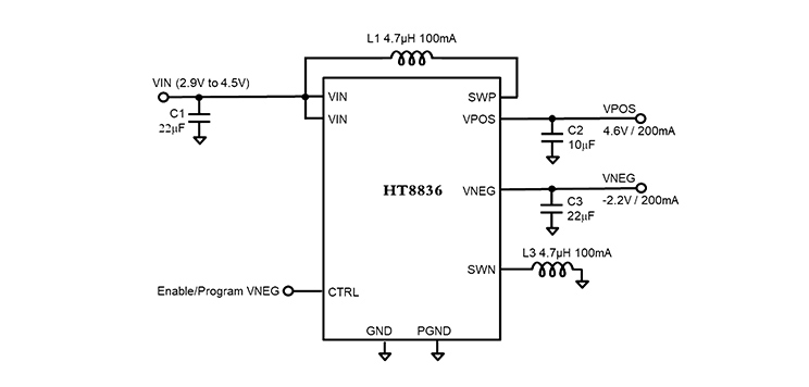
3. Typical Application Circuit Diagram
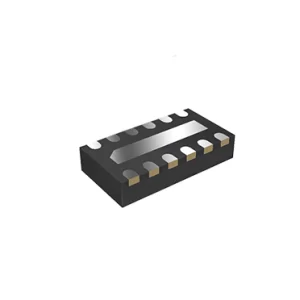
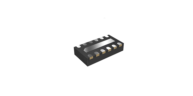
4. Pin Diagram and Functional Description
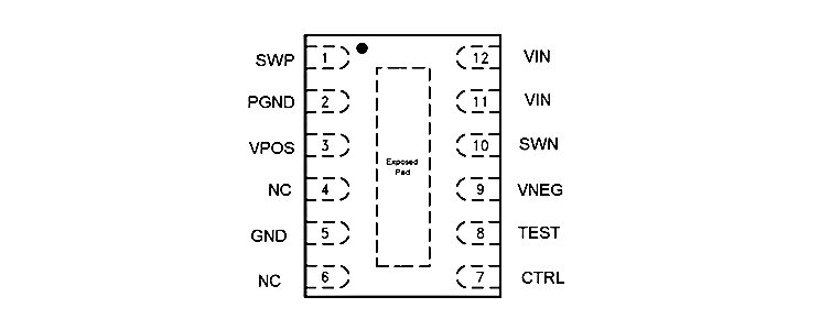
| Pin Name | Pin Number | Functional Description |
| SWP | 1 | Boost Converter (VPOS) Switch Pin |
| PGND | 2 | Boost Converter (VPOS) Power Ground |
| VPOS | 3 | Boost Converter (VPOS) Output |
| NC | 4 | Reserved Pin, Not Connected |
| GND | 5 | Ground |
| NC | 6 | Reserved Pin, Not Connected |
| CTRL | 7 | Boost Converter (VPOS) and VNEG Enable/Program Pin |
| TEST | 8 | Reserved for Device Testing. Not Connected |
| VNEG | 9 | Inverting Converter Output |
| SWN | 10 | Inverting Converter Switch Pin |
| VIN | 11 | Supply Voltage for the device |
| VIN | 12 | Supply Voltage for the device |
| EPAD | Connect this pad to GND and PGND. |