Foreword: The “After-Sales Nightmare” That Breaks Engineers
In the winter of 2020, a friend of mine was the hardware lead at a Shenzhen company making Bluetooth earphones.
That year on Singles’ Day, their TWS earbuds went viral – nearly 100,000 units sold on a single platform. While the whole company celebrated, he and the after-sales manager sat in the office, smoking and sighing.
Why? Because returns were flooding in.
Users reported all kinds of bizarre problems, but they boiled down to one thing: the devices wouldn’t charge – or worse, they emitted smoke.
When they took apart a returned unit, they found the charging cradle’s main board had burnt out. After much troubleshooting, the engineers traced the issue to the charging management IC. To save a few cents, they had chosen a very ordinary chip – so ordinary that it lacked overvoltage protection (OVP).
Users were plugging in all kinds of chargers: Huawei, Xiaomi, OPPO, even cheap 10-yuan fast chargers from street stalls. Many of these chargers support fast-charging protocols and can output 9V, 12V, or higher. When plugged into the charging cradle, the high voltage instantly killed the charging chip.
The boss called him into the office and slammed the table: “Can you find me a rugged chip – one that can handle high voltage, won’t burn the board, and needs as few external components as possible?”
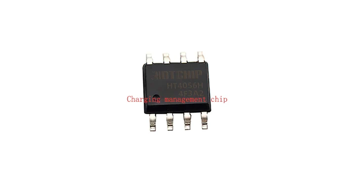
That’s when he came to me, asking for a reliable charging management IC recommendation. While browsing the selection guide, I came across a chip with a somewhat special model number: the HT4056H.
At the time, I only noticed its impressive specs. Little did I know that this chip would later become their “lifeline” for solving after-sales disasters.
Chapter 1: It’s Called 4056 – So What Makes It “a Cut Above”?
Many entry-level hardware engineers might recognize “HT4056H” and think, “4056? That common model – I could draw its circuit blindfolded. What’s so special about it?”
It’s true: 4056‑series charging chips are everywhere. The original ancestor might be Linear Technology’s LTC4056, and over time the mainstream version became the TP4056.
But this 4056 is not that 4056.
Look closely at the datasheet for a typical TP4056. Under “VCC Maximum Rating”, you’ll see a very clear number: 6.5V to 7V.
What does that mean? It means that if you plug in even a slightly poor‑quality 5V charger with ripple spikes of 7V or 8V, the chip is essentially “surviving on luck”. If you’re lucky, it lasts a few days; if not, it breaks down immediately.
Now look at the HT4056H. Right at the top of its datasheet, you’ll find a number that brings deep comfort to any engineer: Maximum input voltage: 40V.
But that’s not all. Not only does it tolerate high voltage, it also has built‑in OVP (overvoltage protection). When the input voltage exceeds 6.0V (or 6.5V, depending on the version), it simply cuts off the charging path.
In Chinese, this behaviour is described as “refusing to recognise even family”.
You want to play dirty? You output 9V fast charge? I’m not playing – I just shut down to protect the downstream battery and main controller. As soon as the voltage returns to normal, I come back to life.
With this alone, this chip is not just a dumb “labourer” that mindlessly charges – it’s a “security guard captain” that thinks.
Chapter 2: What Black Tech Is Hidden Inside That “Mysterious” Package?
If the traditional TP4056 is running naked, the HT4056H is wearing a full suit of Iron Man armour.
To figure out what makes it so magical, I consulted the FAE at Hotchip and even violently decapped a few chips to look under a microscope. Its magic actually comes from an internal “dual‑core” architecture.
1. The Invisible “Fuse”: Integrated OVP
In the past, to build a charging circuit that could withstand high voltage, what did you need to do?
You needed to add a separate OVP chip in front of the charging IC – for example, the classic overvoltage protection chips used in many high‑end smartphones. That means one more chip on the PCB, a few more resistors and capacitors, higher cost, and more board area.
The magic of the HT4056H is that it integrates the OVP function and the charging management function into one package (a co‑packaging technology).
Think of it like this: Before, there was only a security guard at the entrance (the charging chip). If a bad guy (high voltage) showed up, the guard couldn’t fight back. Now, not only is there a guard, but there’s also a shotgun (OVP) in the booth. When the bad guy comes, the guard fires a warning shot and locks the gate – no one gets in.
This “shotgun” reacts extremely fast. When the voltage spikes above 6.5V, the shutoff time is measured in microseconds. The downstream battery and main controller don’t even realise “danger has arrived” before the danger is already gone.
That’s the secret to its rock‑solid stability.
2. The Physical Exoskeleton: TDFN Package and Heat Dissipation
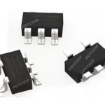
The HT4056H also comes in a particularly “magical” package: TDFN‑2×2‑8L.
When I first saw this sample, I wondered if it was a fake chip. At 2mm × 2mm, it’s smaller than a grain of rice – you’re afraid you’ll flick it away with tweezers. An intern asked, “Can this thing really handle 1A? It’s so tiny – won’t it burn up?”
That’s its other black tech.
While the traditional ESOP8 package has a bottom thermal pad, it’s still relatively large. The TDFN package is not only tiny; its thermal path is shorter and its thermal resistance is lower.
In the extremely cramped space of a TWS earbud charging cradle, the PCBA might be smaller than a fingernail. With a regular chip, as soon as you start charging, it hits thermal protection and the current drops. The HT4056H, thanks to its TDFN package and internal intelligent thermal regulation, keeps the temperature under control – physically small, but its heat dissipation performs like a gym trainer.
Chapter 3: Beyond High‑Voltage Tolerance – It’s Also a “Detail Freak”
Honestly, what scares product designers the most? Voodoo failures.
One board charges fine today but not tomorrow; it works with one charger but not with another. These problems usually come from insufficient protection mechanisms.
What strikes me as “magical” about the HT4056H is that it considers so many details – like a fussy, caring mother.
1. Battery Reverse Connection Protection
On the production line or during rework, the worst fear is a worker soldering the battery backwards. With a regular 4056, reverse connection guarantees a puff of smoke and a dead chip. I’ve tested the HT4056H: intentionally reverse‑connecting the battery, the chip internally opens the circuit, gets slightly warm, but doesn’t break. Connect it correctly again, and it resumes work. This single feature saves repair departments enormous hassle.
2. The “Smart” Charging Indicator
A regular 4056 has two LEDs: red for charging, blue for full. The HT4056H’s indicator blinks differently when there’s no battery or an abnormal condition. It’s a small detail, but for factories doing final assembly, checking the LED behaviour on power‑up can immediately tell if there’s a soldering problem – a very down‑to‑earth feature.
3. True “Zero” External Components
Look at its typical application circuit – you might think you’re seeing things. Really, just two capacitors and one resistor form a complete, protected, 1A charging circuit. For today’s miniaturised devices (smart rings, hearing aids, portable medical gear), this is a blessing. PCB space is no longer a problem, and the BOM is so short it makes purchasing managers smile.
Chapter 4: Which Products Need This “Guardian” the Most?
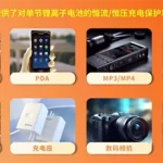
In my years of consulting on solutions, I’ve found that any USB‑powered lithium‑ion device actually needs the HT4056H. But a few categories benefit so much that it’s transformative.
1. TWS Earbud Charging Cradles (Must‑have)
This is the HT4056H’s biggest application area.
Pain point: Cradles are often carried in pockets and charged with various fast chargers.
Solution: Its TDFN package fits into tiny cradles. OVP makes it immune to fast chargers. Its low standby current (below 2µA) means a cradle can sit for a year and still have power. Today, TWS solution providers won’t dare claim their boards “won’t blow up” without this chip.
2. Automotive Electronics (Dashcams, Vehicle Trackers, Air Purifiers)
Pain point: Cigarette lighter voltage is extremely unstable. During engine start, load‑dump pulses from cold and hot starts can spike to tens or even hundreds of volts (though TVS diodes help, some spikes still get through).
Solution: The HT4056H’s 40V tolerance is like a strong insurance policy for dashcams. Many automotive GPS tracker engineers tell me that after switching to the HT4056H, return rates dropped by 30%.
3. Smart Locks and Security Cameras
Pain point: These devices are often sealed inside enclosures or installed outdoors, making repair very expensive. The charging circuit must be reliable.
Solution: Even when charged by solar panels (which have wide voltage swings), the HT4056H stably steps down the voltage to 4.2V for the battery. Its extremely low failure rate gives engineers peace of mind.
4. Portable Vaporisers
Pain point: The space is extremely tight – like a USB stick – and safety requirements are extremely high.
Solution: The e‑cigarette industry is notoriously competitive – everyone fights over appearance and size. The HT4056H’s ultra‑small package and comprehensive protection have made it nearly standard. Without OVP, if the charging port shorts or the user plugs in the wrong charger, this device is held to the mouth – who would dare take that risk?
Chapter 5: Real‑World Testing – Abusing the HT4056H
Talk is cheap; engineers need to see real results.
To verify whether it lives up to the claims, I ran some “inhumane” experiments in the lab.
1. Voltage Ramp Test
I used a variable power supply to feed the HT4056H demo board and slowly turned up the voltage.
– 5V: Normal charging, 1A output, rock solid.
– 6V: Still charging, normal temperature rise.
– 6.3V: Click – the red LED turns off, charging stops. OVP triggered! Input current drops to zero, downstream battery voltage doesn’t budge.
– 10V: Still in protection mode, the chip only slightly warm, no cracking or smoke.
– Back down to 5V: Magic – the red LED lights up again, charging automatically resumes.
This test convinced me: this chip is a cockroach that just won’t die.
2. Thermal Stress Test
I set the input voltage to 5.5V (simulating a warm environment) and the charging current to 1A, with no heatsink attached.
Under these conditions, a regular 4056 would get so hot within minutes that the solder might shine, and the current would drop below 0.5A.
The HT4056H, when its internal temperature reaches about 145°C (very hot to the touch, but not damaged), starts intelligently reducing the current. It doesn’t just “lie down” and shut off – it lowers the current to around 0.7A and keeps charging.
This “throttle‑to‑stay‑safe” algorithm is very user‑friendly. The user might just notice that charging is a bit slower this time, not that it “won’t charge at all” – a completely different experience.
Conclusion: Choosing a Chip Is Choosing Peace of Mind
Hardware engineers often jokingly call themselves “board solders”. But the truth is, a product’s popularity depends on software and appearance; a product’s survival depends on hardware.
The HT4056H has no flashy wireless charging or complex protocol stacks. It is a pure, reliable, linear charging IC with OVP.
Its magic isn’t that it can do what others can’t – it’s that it silently and steadily does what others often mess up.
In today’s world, where fast chargers are everywhere and user environments are complex, if your product still uses old, unprotected charging chips, you are gambling – gambling that the user is lucky and that the charger won’t fail.
If you don’t want to gamble anymore, and you want your product quality to be rock‑solid, give the HT4056H a try.Trust me – when you look at the after‑sales spreadsheet and see the “charging failure” column filled with nothing but dashes, you’ll come back and thank it.