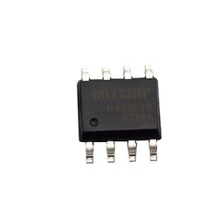
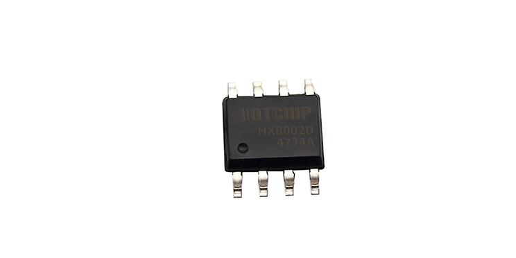
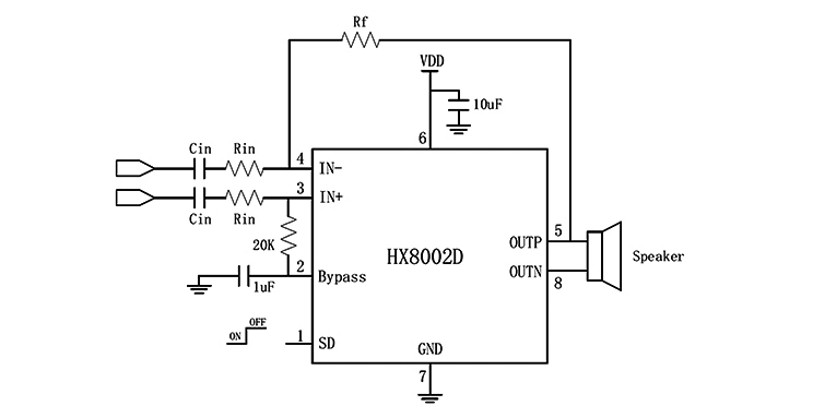
The differential input architecture of the HX8002D effectively enhances noise suppression capabilities. The product features a simple application circuit that requires only a minimal number of external components while delivering high-quality, low-distortion output.
The HX8002D includes a shutdown function, significantly extending system standby time. Its overheat protection feature enhances system reliability, while the POP noise suppression function improves auditory experience and simplifies system debugging. The HX8002D is available in an SOP8 package.
1. Specifications
Unless otherwise specified, VDD = 5V, gain = 20dB, RL = 8Ω, and T = 25°C.
| Symbol | Parameters | Condition | Min. | Typ. | Max. | Unit | |
| Po | Output Power | THD+N=10%, f=1KHZ, RL=8Ω | VDD=5.0V | 1.6 | W | ||
| VDD=4.2V | 1.1 | ||||||
| VDD=3.7V | 0.85 | ||||||
| THD+N=1%, f=1KHZ, RL=8Ω | VDD=5.0V | 1.3 | W | ||||
| VDD=4.2V | 0.86 | ||||||
| VDD=3.7V | 0.66 | ||||||
| THD+N=10%, f=1KHZ, RL=4Ω | VDD=5.0V | 2.6 | W | ||||
| VDD=4.2V | 1.7 | ||||||
| VDD=3.7V | 1.3 | ||||||
| THD+N=1%, f=1KHZ, RL=4Ω | VDD=5.0V | 2.0 | W | ||||
| VDD=4.2V | 1.3 | ||||||
| VDD=3.7V | 1.0 | ||||||
| THD+N=10%, f=1KHZ, RL=3Ω | VDD=5.0V | 2.8 | W | ||||
| VDD=4.2V | 1.95 | ||||||
| VDD=3.7V | 1.46 | ||||||
| THD+N=1%, f=1KHZ, RL=3Ω | VDD=5.0V | 2.0 | W | ||||
| VDD=4.2V | 1.5 | ||||||
| VDD=3.7V | 1.1 | ||||||
| THD+N | Total Harmonic Distortion + Noise | VDD=5.0V, PO=1.0W, RL=8Ω | f=1KHz | 0.3 | % | ||
| VDD=3.7V, PO=0.5W, RL=8Ω | 0.4 | ||||||
| GV | Gain | Rin=27K,Rf=150K | VDD=3.7V | 20 | dB | ||
| PSRR | Power Supply Rejection Ratio | VDD=4.2V ±200mVp-p | f=1KHz | 57 | dB | ||
| SNR | Signal-to-Noise Ratio | VDD=5.0V, Vorms=1V, GV=20dB | f=1KHz | 87 | dB | ||
| Vn | Residual Noise | VDD=5.0V, Input floating with Cin=0.1μF | A-weighting | 35 | μV | ||
| No A-weighting | 53 | ||||||
| Dyn | Dynamic Range | VDD=5.0V, THD=1% | f=1KHz | 97 | dB | ||
| IQ |
Quiescent Current |
VDD=5.0V | VSD=0.3V No Load | 5.5 | mA | ||
| VDD=4.2V | 4.5 | ||||||
| VDD=3.7V | 3.5 | ||||||
| ISD | Shutdown Current | VDD=2.0V to 5.0V | VSD=3.3V | 1 | μA | ||
| Vos | Offset Voltage | VDD=5V, AC_GND | 3 | mV | |||
| Tst | Start-up Time | CByp =1.0uF | 90 | mS | |||
| OTP | Thermal Protection | Junction Temperature, No Load | VDD=5.0V | 175 | ℃ | ||
| OTH | Hysteresis Temperature | 30 | |||||
2. Product Features
- Output Power:
- Operating Voltage: 2.5V to 5.5V.
- Low Distortion and Low Noise.
- Start-up POP Noise Suppression.
- Shutdown Current Less Than 1µA.
- Overheat Protection Function.
3. Functional Block Diagram
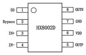
4. Pin Diagram and Functional Description
| Pin Name | Pin Number | I/O | Functional Description | |
| SD | 1 | I | System Shutdown Control, Default High Level (Shutdown at High Level, Operate at Low Level) | |
| Bypass | 2 | I | Reference Voltage | |
| IN+ | 3 | I | Audio Positive Input | |
| IN- | 4 | I | Audio Negative Input | |
| OUTP | 5 | O | Audio Positive Output | |
| VDD | 6 | P | Power | |
| GND | 7 | Ground | ||
| OUTN | 8 | O | Audio Negative Output |
5. Features
- Input Resistance (Ri).
- Input Capacitance (Ci).
- Bypass Capacitor (CBYP).
- Shutdown Operating Mode.
