
1. Specifications
Features (Ta = -40°C to +85°C)
| Symbol | Features | Condition | 1.65V to 3.6V | Unit | ||
| Min. | Typ. | Max. | ||||
| IDPD | Deep Power-Down Current | CS# = Vcc, all other inputs at 0V or Vcc | 0.3 | 3 | uA | |
| ISB | Standby Current | CS# = Vcc, all other inputs at 0V or Vcc | 0.8 | 3 | uA | |
| ICC1 | Low Power Read Current (03h) | f=1MHz; IOUT=0mA | 1 | 1.5 | mA | |
| f=33MHz; IOUT=0mA | 1.6 | 2 | ||||
| ICC2 | Read Current (0Bh) | f=50MHz; IOUT=0mA | 2.2 | 3 | mA | |
| f=85MHz; IOUT=0mA | 2.5 | 3.5 | ||||
| ICC3 | Program Current | CS#=Vcc | 4 | 5 | mA | |
| ICC4 | Erase Current | CS#=Vcc | 4 | 5 | mA | |
| ILI | Input Load Current | All input levels at CMOS | 1 | uA | ||
| ILO | Output Leakage Current | All inputs at CMOS levels | 1 | uA | ||
| VIL | Input Low Voltage | 0.2Vcc | V | |||
| VIH | Input High Voltage | 0.8Vcc | V | |||
| VOL | Output Low Voltage | IOL=100uA | 0.2 | V | ||
| VOH | Output High Voltage | IOH=-100uA | Vcc-0.2 | V | ||
2. Product Features
- Power Supply Range for Read, Erase, and Program: 1.65V to 3.6V.
- Ultra-Low Power Consumption for Read, Erase, and Program.
- x1, x2 Multi I/O Support.
- High Reliability: 100K program/erase cycles endurance and 20-year data retention.
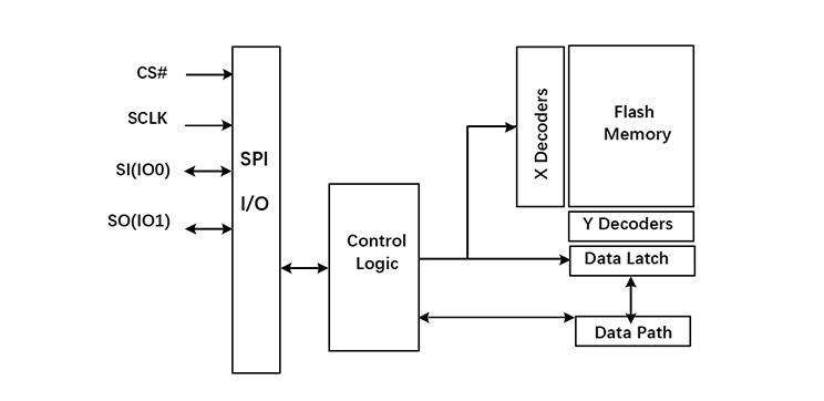
3. Functional Block Diagram
4. Pin Diagram and Functional Description
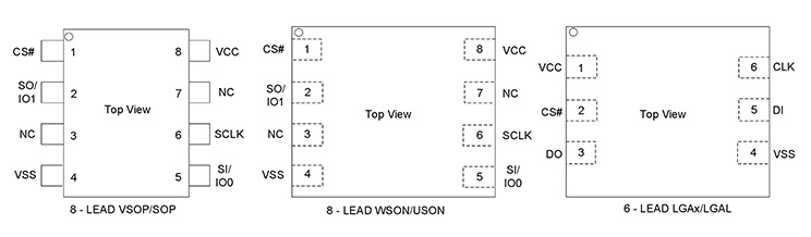
| Pin Name | Pin Number | I/O | Functional Description |
| CS# | 1 | I | Chip Select Input |
| SO (IO1) | 2 | I/O | Data Output (Data I/O1) |
| NC | 3 | No Connect | |
| VSS | 4 | Ground | |
| SI (IO0) | 5 | I/O | Data Input (Data I/O0) |
| SCLK | 6 | I | Serial Clock Input |
| NC | 7 | No Connect | |
| VCC | 8 | Power Supply |