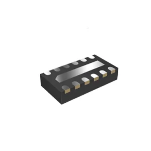
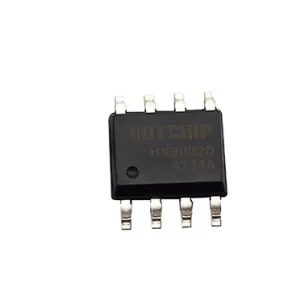
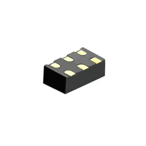
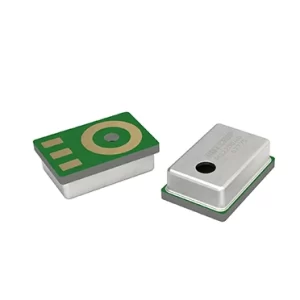
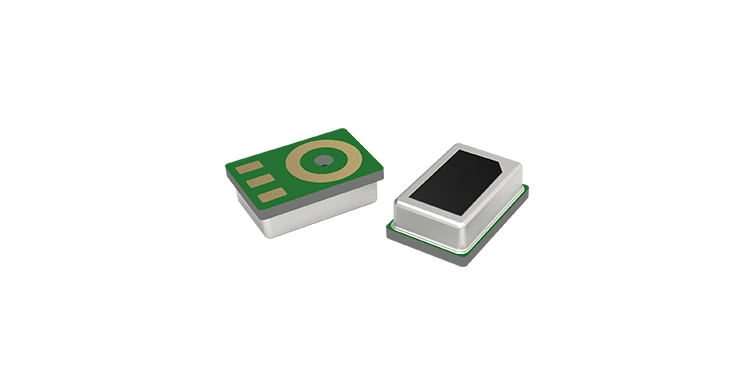
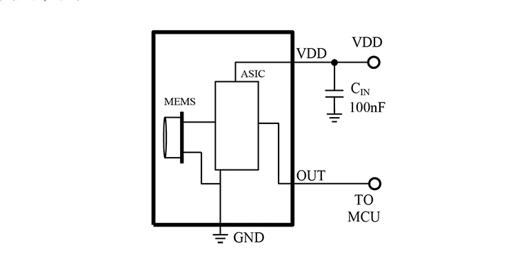
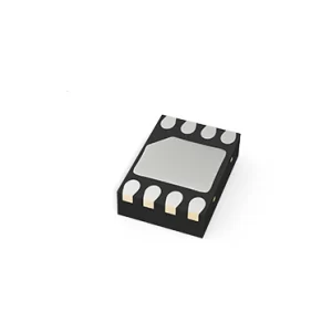
MS2202AB-M10 is a MEMS airflow pressure switch sensor suitable for detecting the smoking status of atomizer. When the built-in MEMS chip senses the change of air pressure, the MEMS chip converts the change of air pressure into the change of capacitance, and the MEMS chip is connected to the input of the built-in capacitive airflow detection ASIC chip to determine the user’s operation behavior through the detection of capacitance change signals by the circuit of ASIC input and output the corresponding trigger high and low level signals. The ASIC input circuit detects the capacitance change signal to determine the user’s operation behavior and outputs the corresponding trigger high and low level signals. With ASIC design, there will not be the current MCU program’s crash phenomenon, nor will there be below the critical voltage caused by the chip can not be reset phenomenon; power-saving mode quiescent current ≤ 5uA, peripheral application circuit is simple.
1. Limited Parameters
| Parameter | Symbol | Min. | Typ. | Max. | Unit |
| Operating Temperature | TOPR | -40 | 85 | ℃ | |
| Storage Temperature | TSTG | -40 | 125 | ℃ | |
| Supply Voltage | Vdd | -0.3 | 5.5 | V | |
| ESD | 2000 | V |
2. Performance Parameters
Unless otherwise specified, the conditions are VDD = 4.0V and TA = 25°C.
| Symbol | Meaning | Condition | Min. | Typ. | Max. | Unit |
| P | Operating Pressure | -100 | -200 | Pa | ||
| VDD | Operating Voltage Range | 2.4 | 5 | V | ||
| IQ | Static Power Consumption | 3 | 5 | uA | ||
| Vol | Output Low Voltage | VDD = 3.7V, Load Resistance = 2.2KΩ | VDD*15% | V | ||
| Voh | Output High Voltage | VDD = 3.7V, Load Resistance = 2.2KΩ | VDD*85% | V | ||
| tFIRE | Startup Delay Time | Time from effective capacitance change to OUT rising | 60 | ms | ||
| tOFF | Off Delay Time | Time from microphone capacitance recovery to OUT falling | 60 | ms | ||
| tBLOW | Reverse Blow Protection Time | Duration of air blowing without triggering activation | 15 | s | ||
| tMAX | Timeout Protection Time | Maximum continuous activation time | 12 | s | ||
| SM | Algorithm Resolution [1] | 1/32 | ||||
| HBM | ESD Protection Capability | 2000 | V |
Note [1]: The theoretical maximum capacitance change rate that the internal algorithm of the chip can resolve. The actual resolution or sensitivity may be affected by external factors such as the PCB layout and surrounding components.
3. Typical Application Circuit Diagram
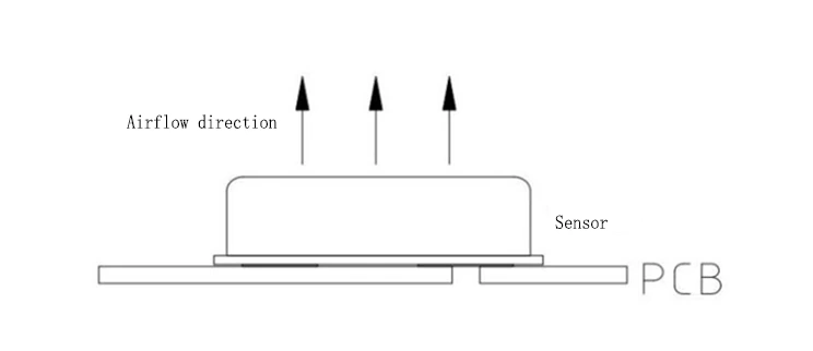
4. System Diagram
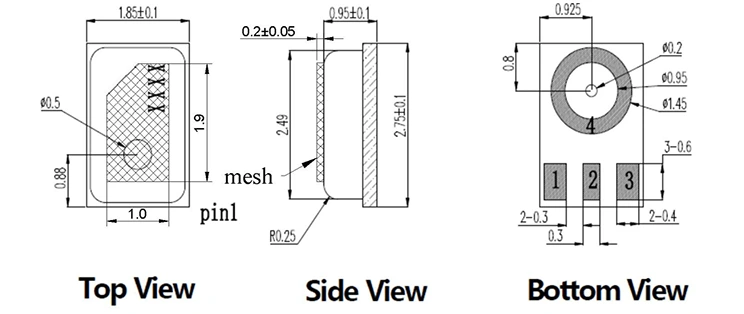
Unit: mm Unmarked Tolerance: ±0.1(mm)
| ltem | Dimension | Tolerance(+/-) | Units |
| Length(L) | 2.75 | 0.1 | mm |
| Width(W) | 1.85 | 0.1 | mm |
| Height(H) | 0.95 | 0.1 | mm |
| Acoustic Port(AP1) | ∅0.2 | 0.05 | mm |
| Acoustic Port(AP2) | ∅0.5 | 0.05 | mm |
| Pin | Pin Name | Description |
| 1 | NC | / |
| 2 | Output | Switch output |
| 3 | VDD | Power supply |
| 4 | GND | Ground |
Note: All Ground Pin must be connected to the ground in end application.
