Huaxin Zhenbang is shifting its focus from “core” development to “new” development, striving to build a new quality and productive force in the semiconductor industry chain. Hotchip Technology.
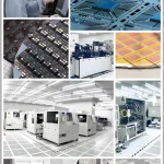
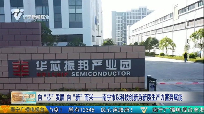
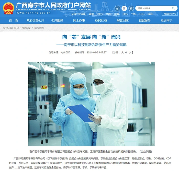
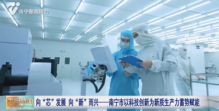
Guangxi Huaxin Zhenbang Semiconductor Co., Ltd. is a joint venture established by Nanning Production and Investment Group Co., Ltd. and Shenzhen Hotchip Technology Co., Ltd. It is a national key development project, and Huaxin Zhenbang is the first integrated circuit wafer level packaging and testing manufacturing project in Guangxi. Many driver circuits for displays, mobile phones, and smart wearable devices are showcased in the enterprise exhibition hall. On every circuit board, the driver chip is not as big as a fingernail, but it is an indispensable “central unit” in electronic devices.
A driver chip can simultaneously handle the power on/off of hundreds or thousands of LEDs, and each driver chip is loaded with thousands of wafer bumps for conductivity. The advanced level of wafer bump manufacturing technology determines whether the driver chip can operate with low power consumption and high efficiency. The driver chip is not large in size, but it can become a key hub for controlling displays. Around this’ center ‘, how to innovate technology and improve processes has become the research and development focus of Huaxin Zhenbang.
Huaxin Zhenbang adheres to the development strategy of “innovation driven” and regards breakthroughs in key technologies as the driving force for sustainable development. Key technologies are independently controllable, making Huaxin Zhenbang a leading enterprise in the semiconductor manufacturing field in Guangxi. At present, the company has formed a monthly production and processing capacity of 10000 12 inch wafers in the first phase, filling the gap in the field of advanced wafer level packaging and testing in the integrated circuit industry in Guangxi, and connecting the industrial chain of integrated circuit wafer level packaging and testing and innovative projects in Nanning.
This year, Huaxin Zhenbang is expected to apply for 12 new patents, striving to achieve more results in the integration of the industrial chain and achieve the goal of expanding into a broader market. We will leverage the resource advantages of enterprises to attract more upstream and downstream cooperative enterprises, including design companies and module manufacturing, to settle in Nanning, helping the capital to build a complete semiconductor industry chain and accelerate the development of new quality productivity.
Convert ‘key variable’ to ‘maximum increment’
From the independently innovated electroplating palladium bump process technology to the new generation of memory products that fill the industry gap, the “key variable” of technological innovation is transforming into the “maximum increment” of industrial transformation and upgrading.
Cui Wenhao, Deputy General Manager of Nanning Production and Investment Group, stated that he will continue to cultivate and strengthen leading enterprises in the global 5G communication RF, memory module, chip production and manufacturing, and chip design industries that have already been put into operation, empower enterprises such as Huaxin Zhenbang and Tektronix Semiconductor, expand the scale of the electronic information industry, create an industrial ecosystem of ‘chip design+packaging testing+module+terminal assembly’, and cultivate more new quality productivity for the high-quality development of Nanning’s economy.
Technological breakthroughs, factor clustering, and industrial “chains” have become inevitable choices for the capital to drive industrial upgrading and shape new quality productivity by bringing innovation to enterprises, industries, and development. Nanning has also formed a new economic cycle of “industry technology innovation finance”, and has embarked on a new path of industrialization with the characteristics of a capital city. Next, Guangxi Huaxin Zhenbang will continue to fully utilize the technological and talent advantages of universities, combined with the company’s industrialization advantages, to cooperate in project cooperation and development, innovation platform construction, talent cultivation, and other aspects, further enhancing the level of scientific and technological innovation and assisting the high-quality development of Guangxi’s semiconductor industry.