Chip Quick Sealing | Jiangsu Huaxin Intelligent Manufacturing Semiconductor participated heavily in the formulation of national semiconductor device standards.
Recently, the 2024 National Semiconductor Device Standard Compilation and Training Conference was held in Xuzhou. Representatives from the National Semiconductor Device Standardization Technical Committee, the National Semiconductor Discrete Device Standardization Sub Technical Committee, and other national semiconductor standard editing units and participating units attended the meeting. At the kick-off meeting, it was mentioned that Jiangsu Huaxing Laser Technology Co., Ltd., Xuzhou Zhineng Semiconductor Co., Ltd., Jiangsu Shangda Semiconductor Co., Ltd., Jiangsu Huaxin Zhizao Semiconductor Co., Ltd., and Xuzhou Xinsijie Semiconductor Technology Co., Ltd. will respectively undertake the revision and development of discrete device standards such as the gallium nitride power device standard revision group, the flexible stretchable standard group (flexible substrate), and the long-term storage and testing method standard group (flexible substrate).
As one of the leading companies in the semiconductor intelligent manufacturing industry, Hotchip Technology has always been committed to promoting the rapid development of intelligence in the semiconductor industry. As a subsidiary of Hotchip Group (Shenzhen Hotchip Technology Co., Ltd.), Jiangsu Hotchip Intelligent Manufacturing Semiconductor Co., Ltd. has joined the work of formulating national semiconductor device standards, fully utilizing the group’s rich semiconductor intelligent manufacturing technology and experience, actively promoting the formulation of national industry standards, and providing hard core empowerment to help upgrade the manufacturing capabilities of the semiconductor industry.

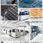
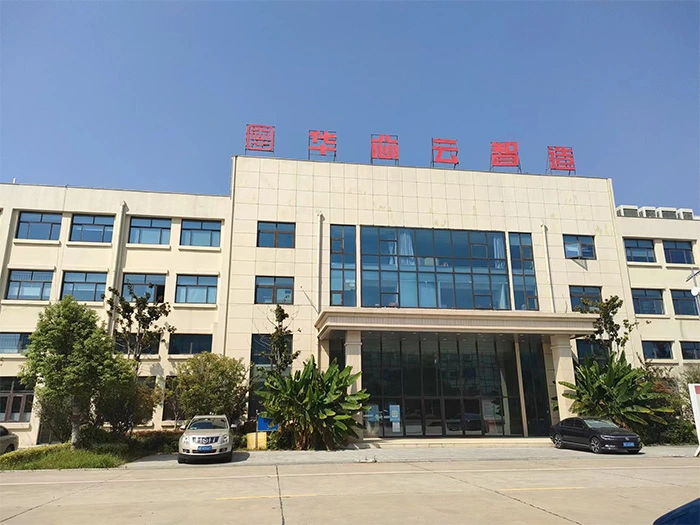
Jiangsu Huaxin Zhizao Semiconductor Co., Ltd. was put into operation in 2020 and continues to operate smoothly, injecting chip packaging and testing capabilities into the group’s UIDM business. It has full process capabilities from wafer testing, grinding and cutting to chip packaging and testing.
The company is located in the Airport Economic Development Zone of Xuzhou City, Jiangsu Province, with a total construction area of 15000 square meters. The company’s business scope includes the production/packaging of semiconductor integrated circuits/semiconductor components, CP testing of wafers, and FT testing of chip products. The business model provides integrated circuit packaging and testing solutions for integrated circuit design enterprises. At present, Jiangsu Huaxin has maintained stable growth for many years. With professional technology and excellent quality, it has won praise from the industry and has become a strategic partner of well-known Fab factories such as Hynix, Eastern, Wanghong, and New Tang. It has long-term stable cooperation with major customers such as Huawei HiSilicon and Jingfeng Mingyuan.
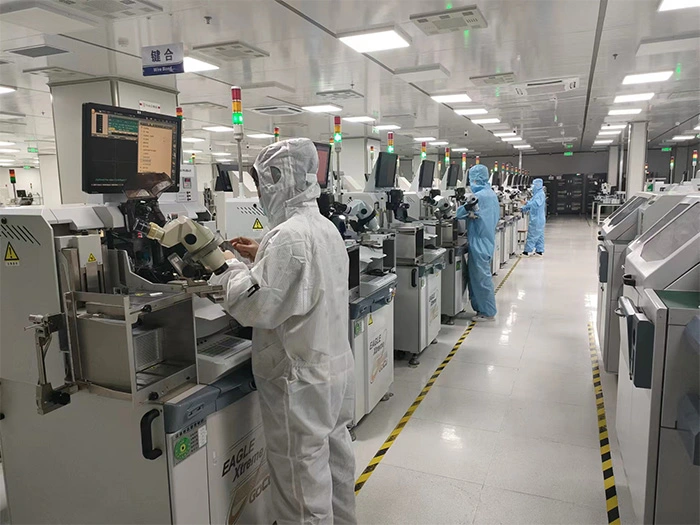
Jiangsu Huaxin Intelligent Manufacturing’s chip packaging and testing business focuses on the fast packaging and testing sampling business and advanced packaging business in the integrated circuit packaging and testing business. The workshop cleanliness level, production equipment, production line layout, process route, technology research and development, business team, and customer introduction are all guided by the fast packaging business. The business development direction is focused on advanced packaging forms such as QFN/DFN, WB-LGA, WB-BGA, FC-BGA, FC-LGA, etc., and focuses on advanced packaging fields such as system level packaging (SiP), high-density fine pitch bump flip chip products (FC products), large-sized/fine pitch flat no pin packaging products (QFN/DFN), etc. It has 9 main packaging forms and a total of over 400 mass-produced varieties.
Integrated circuits are the backbone of the information technology industry, and their technological level and development scale have become important indicators for measuring a country’s industrial competitiveness and comprehensive national strength. Keeping a close eye on industry trends, Xuzhou responds to the wind and “dances” to the forefront, making great efforts to enter the integrated circuit and ICT industries. Starting from 2010, after more than ten years of unremitting efforts, we have achieved industrial scale and agglomeration from scratch and from existing to excellent. In the past three years, we have continuously crossed three levels: 20 billion yuan, 30 billion yuan, and 40 billion yuan.
In recent years, Xuzhou City has focused on the integrated circuit and ICT industries, strengthened semiconductor materials, specialized semiconductor equipment, expanded advanced semiconductor packaging and testing, optimized third-generation semiconductor materials and devices, extended and expanded intelligent terminal applications and intelligent information services, and accelerated the construction of a new highland for the national integrated circuit industry.